- 您现在的位置:买卖IC网 > Sheet目录1905 > ATMEGA8HVA-4CKU (Atmel)MCU AVR 8K FLASH 4MHZ 36-LGA
18
8024A–AVR–04/08
ATmega8HVA/16HVA
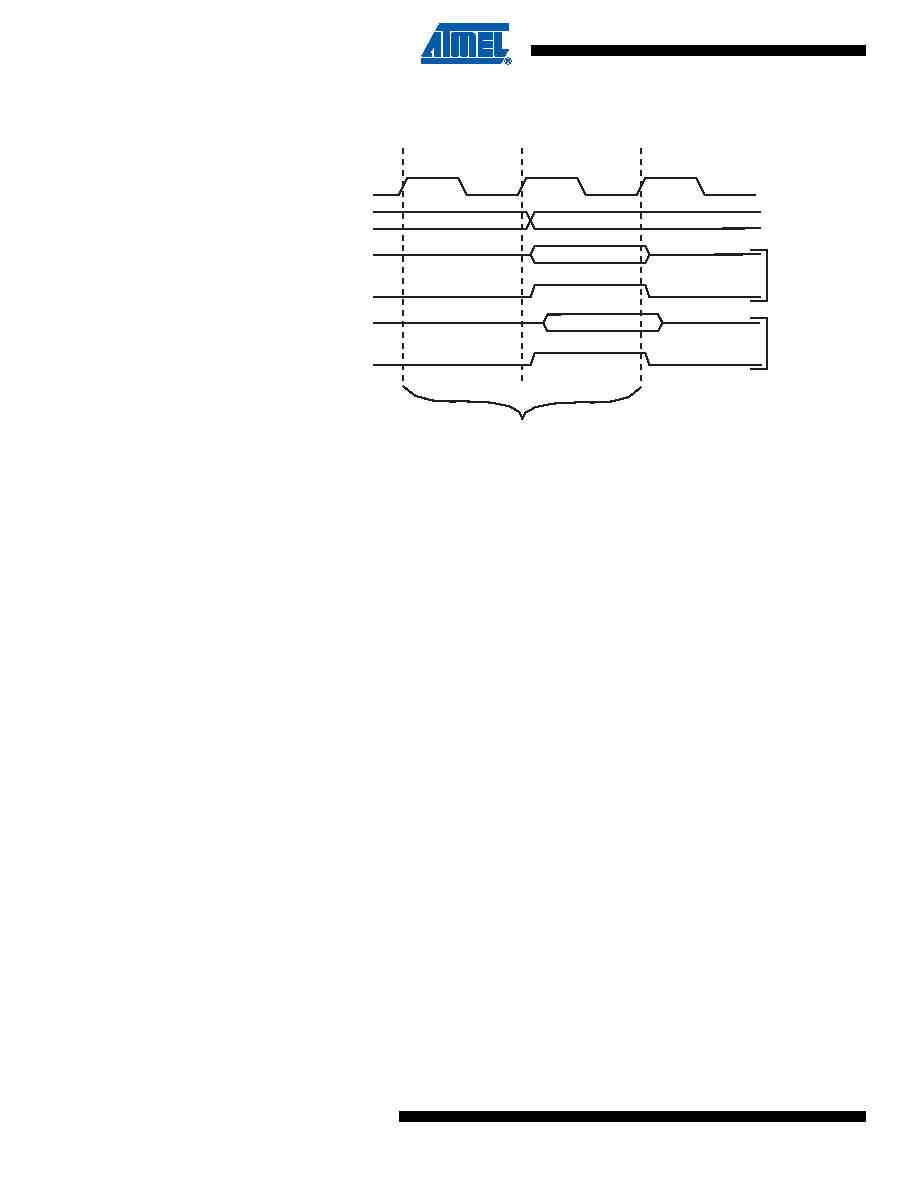
Figure 8-3.
On-chip Data SRAM Access Cycles
8.4
EEPROM Data Memory
The ATmega8HVA/16HVA contains 256 bytes of data EEPROM memory. It is organized as a
separate data space, in which single bytes can be read and written. The EEPROM has an
endurance of at least 100,000 write/erase cycles. The access between the EEPROM and the
CPU is described in the following, specifying the EEPROM Address Registers, the EEPROM
Data Register, and the EEPROM Control Register.
8.4.1
EEPROM Read/Write Access
The EEPROM Access Registers are accessible in the I/O space.
The write access time for the EEPROM is given in Table 8-1 on page 20. A self-timing function,
however, lets the user software detect when the next byte can be written. If the user code con-
tains instructions that write the EEPROM, some precautions must be taken.
In order to prevent unintentional EEPROM writes, a specific write procedure must be followed.
Refer to the description of the EEPROM Control Register for details on this.
When the EEPROM is read, the CPU is halted for four clock cycles before the next instruction is
executed. When the EEPROM is written, the CPU is halted for two clock cycles before the next
instruction is executed.
8.5
I/O Memory
The I/O space definition of the ATmega8HVA/16HVA is shown in ”Register Summary” on page
All ATmega8HVA/16HVA I/Os and peripherals are placed in the I/O space. All I/O locations may
be accessed by the LD/LDS/LDD and ST/STS/STD instructions, transferring data between the
32 general purpose working registers and the I/O space. I/O Registers within the address range
0x00 - 0x1F are directly bit-accessible using the SBI and CBI instructions. In these registers, the
value of single bits can be checked by using the SBIS and SBIC instructions. Refer to the
instruction set section for more details. When using the I/O specific commands IN and OUT, the
clk
WR
RD
Data
Address
Address valid
T1
T2
T3
Compute Address
Read
Wr
ite
CPU
Memory Access Instruction
Next Instruction
发布紧急采购,3分钟左右您将得到回复。
相关PDF资料
ATSAM3N4AA-AU
MCU FLASH 48-QFP
ATSAM3SD8CA-CU
IC MCU 2X256KB CORTEX-M3 100-QFN
ATSAM3U1EB-CU
IC MCU 64KB CORTEX-M3 144-TFBGA
ATSAM3X8EA-CU
IC MCU 2X256KB CORTEX-M3 144-BGA
ATTINY12V-1SUR
IC AVR MCU 1K FLASH 4MHZ 8-SOIC
ATTINY13-20SQR
IC MCU AVR 1KB FLASH 20MHZ 8SOIC
ATTINY13A-MMUR
MCU AVR 1KB FLASH 20MHZ 10DFN
ATTINY13V-10SUR
MCU AVR 1KB FLASH 10MHZ 8SOIC
相关代理商/技术参数
ATMEGA8HVA-4CKUR
功能描述:8位微控制器 -MCU AVR 8KB FLSH 512B EE 1KB SRAM - 4 MHZ RoHS:否 制造商:Silicon Labs 核心:8051 处理器系列:C8051F39x 数据总线宽度:8 bit 最大时钟频率:50 MHz 程序存储器大小:16 KB 数据 RAM 大小:1 KB 片上 ADC:Yes 工作电源电压:1.8 V to 3.6 V 工作温度范围:- 40 C to + 105 C 封装 / 箱体:QFN-20 安装风格:SMD/SMT
ATMEGA8HVA-4TU
功能描述:8位微控制器 -MCU AVR 8KB, 512B EE 4MHz 1KB SRAM 1.8-9V RoHS:否 制造商:Silicon Labs 核心:8051 处理器系列:C8051F39x 数据总线宽度:8 bit 最大时钟频率:50 MHz 程序存储器大小:16 KB 数据 RAM 大小:1 KB 片上 ADC:Yes 工作电源电压:1.8 V to 3.6 V 工作温度范围:- 40 C to + 105 C 封装 / 箱体:QFN-20 安装风格:SMD/SMT
ATMEGA8HVA-4TUR
功能描述:8位微控制器 -MCU AVR 8KB FLSH 512B EE 1KB SRAM - 4 MHZ RoHS:否 制造商:Silicon Labs 核心:8051 处理器系列:C8051F39x 数据总线宽度:8 bit 最大时钟频率:50 MHz 程序存储器大小:16 KB 数据 RAM 大小:1 KB 片上 ADC:Yes 工作电源电压:1.8 V to 3.6 V 工作温度范围:- 40 C to + 105 C 封装 / 箱体:QFN-20 安装风格:SMD/SMT
ATMEGA8HVD-4MX
功能描述:8位微控制器 -MCU AVR 8KB, 512B EE 4MHz 1KB SRAM 2.1-8V
RoHS:否 制造商:Silicon Labs 核心:8051 处理器系列:C8051F39x 数据总线宽度:8 bit 最大时钟频率:50 MHz 程序存储器大小:16 KB 数据 RAM 大小:1 KB 片上 ADC:Yes 工作电源电压:1.8 V to 3.6 V 工作温度范围:- 40 C to + 105 C 封装 / 箱体:QFN-20 安装风格:SMD/SMT
ATMEGA8L-8AC
功能描述:8位微控制器 -MCU AVR 8K FLASH 512B EE 1K SRAM ADC 3V RoHS:否 制造商:Silicon Labs 核心:8051 处理器系列:C8051F39x 数据总线宽度:8 bit 最大时钟频率:50 MHz 程序存储器大小:16 KB 数据 RAM 大小:1 KB 片上 ADC:Yes 工作电源电压:1.8 V to 3.6 V 工作温度范围:- 40 C to + 105 C 封装 / 箱体:QFN-20 安装风格:SMD/SMT
ATMEGA8L8AI
制造商:Atmel Corporation 功能描述:
ATMEGA8L-8AI
功能描述:8位微控制器 -MCU AVR 8K FLASH 512B EE 1K SRAM ADC 3V RoHS:否 制造商:Silicon Labs 核心:8051 处理器系列:C8051F39x 数据总线宽度:8 bit 最大时钟频率:50 MHz 程序存储器大小:16 KB 数据 RAM 大小:1 KB 片上 ADC:Yes 工作电源电压:1.8 V to 3.6 V 工作温度范围:- 40 C to + 105 C 封装 / 箱体:QFN-20 安装风格:SMD/SMT
ATMEGA8L-8AJ
功能描述:IC MCU AVR 8K 5V 8MHZ 32-TQFP RoHS:是 类别:集成电路 (IC) >> 嵌入式 - 微控制器, 系列:AVR® ATmega 标准包装:9 系列:87C 核心处理器:8051 芯体尺寸:8-位 速度:40/20MHz 连通性:UART/USART 外围设备:POR,WDT 输入/输出数:32 程序存储器容量:32KB(32K x 8) 程序存储器类型:OTP EEPROM 大小:- RAM 容量:256 x 8 电压 - 电源 (Vcc/Vdd):4.5 V ~ 5.5 V 数据转换器:- 振荡器型:内部 工作温度:0°C ~ 70°C 封装/外壳:40-DIP(0.600",15.24mm) 包装:管件